
反強磁性体・フェリ磁性体の機能制御:
スピントロニクス
Smaller yet faster?
With a spin that remembers
The Puzzle is solved
シリコン(Si)に代表される半導体を基盤とした現代社会を支えているのは、エレクトロニクスと呼ばれる物質中の電荷を電気的に制御する技術です。一方、電子は電荷のほかに「スピン」(スピン角運動量) Sz=±ħ/2という内部自由度を持ちます。物質中で電子がお互いに強い斥力を感じて局在すると、このスピン自由度が顔を出し、様々な磁性を示すようになります。これらの自由度はそれぞれ異なる物質で現れるため、独立した観点や興味から研究が行われてきました。しかし、近年、薄膜試料作製技術や微細加工技術の向上やスピン流と呼ばれる角運動量の流れの理解が進んだことで、電荷とスピンの2つの自由度を同時に利用したり、スピン自由度のみによる現象を分離したりできる新しいエレクトロニクス技術「スピントロニクス」が大きく進展し注目されています。
巨大磁気抵抗効果(Giant Magnetoresistance : GMR)[Fert と Grünbergは2007年にノーベル賞を受賞]やトンネル磁気抵抗効果(Tunnel Magnetoresistance : TMR)の発見を契機に、スピントロニクス研究は飛躍的な発展をとげ、身近にある磁気記録装置など数多くのデバイスが開発されてきました。例えば、強磁性層/絶縁層/強磁性層の三層を基本とした強磁性トンネル接合素子を用いた磁気抵抗メモリ(Magnetoresistive Random Access Memory : MRAM)は、磁化の向きを単位として不揮発に情報を記憶することが可能で、既存の半導体技術を用いた揮発性メモリを各段に省エネルギー化できるため、大きな注目を集めています。スピントロニクスの研究に用いられる物質は金属、半導体、絶縁体と多岐にわたります。そのなかでも、特に研究が盛んに行われているのが強磁性金属です。代表的なものとしては、FeやCo、Niなどが知られていますが、最近では複数の元素からなるホイスラー合金等の金属間化合物にも研究対象が広がってきています。強磁性体では磁化が秩序変数であるために、その大きさに比例して電気や光、熱などに対しての巨大な応答を得ることができます。また、この巨大応答を駆使することで、多くのスピントロニクスデバイスが開発されてきました。
これからのIoT時代のBig DataをAIで処理する際など、超高密度・超高速駆動のメモリが必要となるシーンはますます増える一方です。現在、スピントロニクスで用いられている材料の多くは強磁性体ですが、磁気デバイスの更なる高性能化への期待から、最近では反強磁性体が主に次世代メモリとして検討されています。それは反強磁性体が、以下の理由から、超高密度・超構造駆動のメモリを実現するのに最適と考えられるからです。すなわち、反強磁性体のメリットは、
-
磁化がゼロ、あるいは、極端に小さいため、漏れ磁場が小さい。そのため、高密度化に有利。
-
スピンの歳差運動の周波数がTHz程度とGHz程度の周波数を持つ強磁性体に比べ桁違いに高い。そのため、情報の高速処理に有利。
-
種類が多いために、安全安価な材料で、高密度、高速駆動可能なデバイスを作れる可能性が高い。
などがあげられます。一方で、その開発を大きく妨げてきたのは、磁化を持たない反強磁性体を用いる上で「磁気構造由来の巨大応答を得ることとその制御が困難である」点でした。
我々の研究室では、従来のスピントロニクスで用いられていた強磁性体の磁化や磁気双極子ではなく、より高次の磁気秩序変数である「磁気多極子」[1]やディラックやワイル粒子をはじめとする「トポロジカル電子構造」に着目をし、反強磁性体をはじめとした物質における新奇量子多体現象の開拓をおこなっています。最近では、運動量空間に存在するワイル点由来のベリー曲率[2]に由来した巨大な異常ホール効果[3,4]や異常ネルンスト効果[5]など、従来の反強磁性体では不可能と思われてきた電気[3,4]や熱[5]、光[6]などに対しての巨大な応答を室温で得ることに世界で初めて成功しています。
またスピントロニクス技術を基軸とした表面や界面物性の開拓[7,8]に特に注力しており、非磁性重金属と反強磁性ワイル金属との界面に生じるスピン流による反強磁性秩序やワイル点を電気的に制御する手法[9,10]や不揮発性メモリ応用に必須の読み出し手法であるトンネル磁気抵抗効果[11]の実証にも成功しています。
その他にも、ナノ粒子におけるトポロジカル電子機能の発現[12]や交換バイアス効果による局所的な磁気秩序の制御[13]、脳形計算にもつながる新原理の多値記録手法の原理検証[14]などにも成功しています。これらの成果は、反強磁性体スピントロニクスを実現する基盤技術として世界的に注目されています。
このように我々の研究室においては、物質の持つ電気的・磁気的性質をミクロな観点から理解し、それらの量子多体現象としての新しい可能性を追求しながら、基礎から応用に直結する波及効果の高い研究の構築を目指しています[15]。
[1] M.-T. Suzuki et al., Phys. Rev. B 95, 094406 (2017).
[2] K. Kuroda, T. Tomita et al., Nat. Mater. 16, 1090 (2017).
[3] S. Nakatsuji, N. Kiyohara, and T. Higo, Nature 527, 212 (2015).
[4] N. Kiyohara, T. Tomita, and S. Nakatsuji, Phys. Rev. Applied 5, 064009 (2016).
[5] M. Ikhlas, T. Tomita et al., Nat. Phys. 13, 1085 (2017).
[6] T. Higo et al., Nat. Photon. 12, 73 (2018).
[7] T. Higo et al., Appl. Phys. Lett. 113, 202402 (2018). (Featured article)
[8] D. Qu et al., Phys. Rev. Mater. 2, 102001(R) (2018). (Editors' suggestion)
[9] H. Tsai, T. Higo et al., Nature 580, 608 (2020).
[10] T. Higo, K. Kondou et al., Nature 607, 474 (2022).
[11] X. Chen, T. Higo, K. Tanaka et al., Nature 613, 490 (2023).
[12] T. Matsuo et al., Appl. Phys. Lett. 121, 013103 (2022).
[13] M. Asakura et al., Adv. Mater. XX, 2400301 (2024).
[14] T. Higo et al., Adv. Funct. Mater. 31, 2008971 (2021).
[15] 肥後, 田中, 中辻, 数理科学 2024年5月号.
研究ハイライト
Magnetic Field Switching of Exchange Bias in a Metallic FM/AFM Heterostructure at Room Temperature
M. Asakura, T. Higo, T. Matsuo, Y. Tsushima, S. Kurosawa, R. Uesugi, D. Nishio-Hamane, S. Nakatsuji, Nano Lett. 25, 10294 (2025).
The exchange bias effect, which causes a shift in the ferromagnetic hysteresis loop due to magnetic coupling with an adjacent antiferromagnetic layer, has been a key area of study for fundamental research and spintronic applications. This effect is known to be static once established through a field cooling procedure and is difficult to manipulate isothermally. Here we present the first room temperature field switching of interlayer magnetic coupling at the metallic heterointerface between a ferromagnet and antiferromaget. Specifically, we demonstrate that the exchange bias can be systematically switched by manipulating the global time-reversal-symmetry-broken antiferromagnetic order of Mn3Sn via both magnetic field sweeping and field cooling. Furthermore, we confirm that the magnitude and sign of the interlayer coupling can be tuned by selecting the ferromagnet. These findings provide a novel approach for controlling the magnetic state of ferromagnets and functional antiferromagnets, paving the way for advancing spintronic technologies using antiferromagnets.

© 2025 The Authors. Published by American Chemical Society
Decoding the magnetic bit positioning error in a ferrimagnetic racetrack
M. Ishibashi, M. Kawaguchi, Y. Hibino, K. Yakushiji, A. Tsukamoto, S. Nakatsuji, M. Hayashi, Sci. Adv. 10, eadq0898 (2024).
Current-driven motion of magnetic domain walls is one of the key technologies for developing storage class memory devices. Extensive studies have revealed a variety of material systems that exhibit high-speed and/or lower power propagation of the domain walls driven by electric current. However, few studies have assessed the reliability of the operations of the memory technology. Here, we decode the errors associated with writing and shifting domain walls using nanosecond current pulses in a ~5-micrometer-wide wire composed of a Pt/GdFeCo bilayer. We find that writing a domain wall at the edge of the wire causes a bit positioning error of ~0.3 micrometers, whereas the shifting process induces an error of ~0.1 micrometers per a 2-nanosecond-long current pulse. The error correlation among successive shifting is negligible when the current drive is sufficiently large. These features allow reliable operation of highly packed domain walls in a ferrimagnetic racetrack.


© 2024 The Authors.
Observation of Omnidirectional Exchange Bias at All-Antiferromagnetic Polycrystalline Heterointerface
M. Asakura, T. Higo, T. Matsuo, R. Uesugi, D. Nishio-Hamane, S. Nakatsuji, Adv. Mater. 2400301 (2024).
Due to promising functionalities that may dramatically enhance spintronics performance, antiferromagnets are the subject of intensive research for developing the next-generation active elements to replace ferromagnets. In particular, the recent experimental demonstration of tunneling magnetoresistance and electrical switching using chiral antiferromagnets has sparked expectations for the practical integration of antiferromagnetic materials into device architectures. To further develop the technology to manipulate the magnetic anisotropies in all-antiferromagnetic devices, it is essential to realize exchange bias through the interface between antiferromagnetic multilayers. Here, the first observation on the omnidirectional exchange bias at an all-antiferromagnetic polycrystalline heterointerface is reported. This experiment demonstrates that the interfacial energy causing the exchange bias between the chiral-antiferromagnet Mn3Sn/collinear-antiferromagnet MnN layers is comparable to those found at the conventional ferromagnet/antiferromagnet interface at room temperature. In sharp contrast with previous reports using ferromagnets, the magnetic field control of the unidirectional anisotropy is found to be omnidirectional due to the absence of the shape anisotropy in the antiferromagnetic multilayer. The realization of the omnidirectional exchange bias at the interface between polycrystalline antiferromagnets on amorphous templates, highly compatible with existing Si-based devices, paves the way for developing ultra-low power and ultra-high speed memory devices based on antiferromagnets.

© 2024 The Authors.
Fabrication of single-crystalline YFeO3 films with large antiferromagnetic domains
C. Wang, M. Lippmaa, S. Nakatsuji, J. Appl. Phys. 135, 113901 (2024).
The antiferromagnetic orthoferrite YFeO3 possesses fascinating magnetic properties for spintronics, such as terahertz spin dynamics, ultrafast domain wall motion, and long magnon decay length. YFeO3 belongs to a special family of antiferromagnets that show an unusually strong non-trivial Kerr response due to its weak ferromagnetism. The highly stable antiferromagnetic domains without any spontaneous spin rotation transitions below the 645 K Néel temperature may be useful for nanoscale device applications. We report the successful fabrication of high-quality twinning-free (110)-oriented YFeO3 films by pulsed laser deposition. Detailed structural and magnetic characterization revealed that the crystal structure and magnetic properties of the YFeO3 films are comparable to bulk single crystals. We show that the spin rotation under high magnetic fields follows the two-sublattice approximation model. The film surface is atomically flat with step-terrace surface morphology. A longitudinal magneto-optic Kerr (MOKE) rotation of 10 mdeg was observed at room temperature, which is consistent with earlier reports on bulk single crystals. The in-plane anisotropy of the Kerr response corresponds to the obtained magnetic anisotropy from the SQUID measurement. The large MOKE signal enables the imaging of antiferromagnetic domains and their reversal. The domain size was found to be larger than 100 μm. These high-quality YFeO3 thin films facilitate the fabrication of antiferromagnetic spintronic devices and provide a convenient platform for studying various spin-related phenomena in thin films and at interfaces.

© 2024 Author(s). All article content, except where otherwise noted, is licensed under a Creative Commons Attribution-NonCommercial 4.0 International (CC BY-NC) license
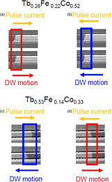
Reversal of current-induced domain wall motion in TbFeCo ferrimagnetic thin films across the magnetization compensation point
M. Ishibashi, K. Yakushiji, M. Kawaguchi, A. Tsukamoto, S. Nakatsuji, M. Hayashi, Jpn. J. Appl. Phys. 62, 013001 (2023).
We report on a systematic investigation of current-induced domain wall motion in TbFeCo ferrimagnetic thin films with a Pt underlayer. The Tb concentration of the alloy is varied to study the effect of the magnetization compensation on the current-induced motion of domain walls. We find that the direction in which domain walls move changes when the Tb concentration crosses the magnetization compensation point. Interestingly, the domain walls move along (against) the current flow for FeCo-rich (deficient) films. When the film composition is slightly Tb-rich than the magnetic compensation point, the domain wall moves along the current at a lower current but reverses its direction when the current is increased. These results suggest that two competing torques act on the domain walls in the Tb-based ferrimagnets (TbFeCo), causing the domain wall velocity to be more than one order of magnitude smaller than that of Gd-based ferrimagnets.

© 2023 The Japan Society of Applied Physics
Piezomagnetic switching of the anomalous Hall effect in an antiferromagnet at room temperature
M. Ikhlas, S. Dasgupta, F. Theuss, T. Higo, S. Kittaka, B. J. Ramshaw, O. Tchernyshyov, C. W. Hicks, S. Nakatsuji, Nat. Phys. 18, 1086 (2022).
Piezomagnetism couples strain linearly to magnetic order, implying that it can produce and control magnetization. However, unlike magnetostriction, which couples magnetization quadratically to strain, it enables bidirectional control of a net magnetic moment. If this effect becomes large at room temperature, it may be technologically relevant, similar to its electric analogue, piezoelectricity. However, current studies of the piezomagnetic effect have been primarily restricted to antiferromagnetic insulators at cryogenic temperatures. Here we report the observation of large piezomagnetism in the antiferromagnetic Weyl semimetal Mn3Sn at room temperature. This material is known for its nearly magnetization-free anomalous Hall effect. We find that a small uniaxial strain on the order of 0.1% can control both the sign and size of the anomalous Hall effect. Our experiment and theory show that the piezomagnetism can control the anomalous Hall effect, which will be useful for spintronics applications.

© The Author(s), under exclusive licence to Springer Nature Limited 2022
Perpendicular full switching of chiral antiferromagnetic order by current
T. Higo, K. Kondou, T. Nomoto, M. Shiga, S. Sakamoto, X. Chen, D. Nishio-Hamane, R. Arita, Y. Otani, S. Miwa, S. Nakatsuji, Nature 607, 474 (2022).
Electrical control of a magnetic state of matter lays the foundation for information technologies and for understanding of spintronic phenomena. Spin–orbit torque provides an efficient mechanism for the electrical manipulation of magnetic orders. In particular, spin–orbit torque switching of perpendicular magnetization in nanoscale ferromagnetic bits has enabled the development of stable, reliable and low-power memories and computation. Likewise, for antiferromagnetic spintronics, electrical bidirectional switching of an antiferromagnetic order in a perpendicular geometry may have huge impacts, given its potential advantage for high-density integration and ultrafast operation. Here we report the experimental realization of perpendicular and full spin–orbit torque switching of an antiferromagnetic binary state. We use the chiral antiferromagnet Mn3Sn (ref. 17), which exhibits the magnetization-free anomalous Hall effect owing to a ferroic order of a cluster magnetic octupole hosted in its chiral antiferromagnetic state. We fabricate heavy-metal/Mn3Sn heterostructures by molecular beam epitaxy and introduce perpendicular magnetic anisotropy of the octupole using an epitaxial in-plane tensile strain. By using the anomalous Hall effect as the readout, we demonstrate 100 per cent switching of the perpendicular octupole polarization in a 30-nanometre-thick Mn3Sn film with a small critical current density of less than 15 megaamperes per square centimetre. Our theory reveals that the perpendicular geometry between the polarization directions of current-induced spin accumulation and of the octupole persistently maximizes the spin–orbit torque efficiency during the deterministic bidirectional switching process. Our work provides a significant basis for antiferromagnetic spintronics.

© The Author(s), under exclusive licence to Springer Nature Limited 2022
Anomalous Hall effect in nanoscale structures of the antiferromagnetic Weyl semimetal Mn3Sn at room temperature
T. Matsuo, T. Higo, D. Nishio-Hamane, S. Nakatsuji, Appl. Phys. Lett. 121, 013103 (2022).
The magnetic Weyl semimetallic state in the chiral antiferromagnet Mn3Sn has attracted interest for its potential in memory technology. Despite vanishingly small magnetization, the material exhibits large transverse responses that can be electrically manipulated, similar to ferromagnets. Through deposition on heated Si/SiO2 substrates, we have fabricated polycrystalline Mn3Sn films that have coarse surfaces, the thinner of which have a discontinuous structure comprised of grains with diameters of the order of 100 nm. We confirm that these grains retain the anomalous Hall effect arising in the time reversal symmetry broken chiral antiferromagnetic phase of Mn3Sn at room temperature by serially connecting the grains with an additional conducting layer. These results pave the path for the potential applications of nanoscale Mn3Sn systems, which could be useful in the development of energy efficient memory devices.


© 2022 Author(s). Published under an exclusive license by AIP Publishing.
Large Hall Signal due to Electrical Switching of an Antiferromagnetic Weyl Semimetal State
H. Tsai, T. Higo, K. Kondou, S. Sakamoto, A. Kobayashi, T. Matsuo, S. Miwa, Y. Otani, S. Nakatsuji, Small Sci. 1, 2000025 (2021).
Developing a technology to electrically manipulate a Weyl semimetal state is a vital step for designing a nonvolatile memory using topologically robust properties. Recently, such manipulation is realized for the first time in the antiferromagnetic Weyl semimetal Mn3Sn using the readout signal of anomalous Hall effect in the Mn3Sn/heavy metal (Pt, W) heterostructures. Here, it is reported that the switching of Hall signal can be significantly enhanced by 1) removing the buffer layer of Ru to adjust the crystal orientation of Mn3Sn, and 2) annealing after deposition of the heavy metal to change the interfacial condition. The switching of the Hall resistance is 0.35 Ω in the Mn3Sn/W sample, which becomes one order of magnitude larger than the previously reported value using Ru/Mn3Sn/Pt heterostructures. Moreover, by increasing the read current, it is found that the readout voltage may go well beyond 1 mV, a milestone for future applications in memory technology.

© 2021 The Authors. Small Science published by Wiley-VCH GmbH