東京大学大学院 理学系研究科物理学専攻 理学部物理学科
中辻・酒井 研究室
Department of Physics, Graduate School of Science and Faculty of Science, The University of Tokyo
Nakatsuji・Sakai Laboratory

Antiferromagnetic spintronics for
next-generation ultrafast memory
Smaller yet faster?
With a spin that remembers
The Puzzle is solved
A pressing challenge facing information technology is the simultaneous improvement of electronic devices' processing speed and energy efficiency. Every time one switches on a computer or cellphone, electron charges begin their journey through microprocessors comprising millions of tiny switches, known as transistors. The transistors decide whether electrons can pass or not, thereby communicating using "0" or "1". Over the decades, we have seen the electronic components shrinking in size at an incredibly rapid pace. Yet, this ever-growing trend is approaching its serious physical limit of energy consumption and heat dissipation, calling for new-concept memory and processing devices.
Spintronics is among the top emerging fields for non-volatile logic and memory devices, offering exciting alternatives to conventional electronics by encoding information into the spins of electrons instead of their charges. The spin – a quantum mechanical property of electrons – behaves as little compass needles that can point up, down, or somewhere in between. Even without moving around inside a material, spins can store and process information via its discrete energy states, creating a whole new era of microprocessors. Traditionally focused on ferromagnets, spintronics research is now evolving towards antiferromagnetic materials. The negligible net magnetization of antiferromagnets makes them robust against stray fields, plus their resonance frequency lies in the range of THz, enabling ultrafast writing speed. However, the tiny response of antiferromagnetic materials to external fields represents a major obstacle for their practical applications. We recently discovered unusually large room-temperature anomalous transport effects in antiferromagnetic topological materials, a significant step forward in transferring spintronics concepts to real-life electronic components that are smaller, faster, and more energy efficient.
The following publications tell the in-depth story about how we manipulate the spin dynamics and spin transport of antiferromagnets for next-generation information technologies. Please feel free to check them out.
[1] M.-T. Suzuki et al., Phys. Rev. B 95, 094406 (2017).
[2] K. Kuroda, T. Tomita et al., Nat. Mater. 16, 1090 (2017).
[3] S. Nakatsuji, N. Kiyohara, and T. Higo, Nature 527, 212 (2015).
[4] N. Kiyohara, T. Tomita, and S. Nakatsuji, Phys. Rev. Applied 5, 064009 (2016).
[5] M. Ikhlas, T. Tomita et al., Nat. Phys. 13, 1085 (2017).
[6] T. Higo et al., Nat. Photon. 12, 73 (2018).
[7] T. Higo et al., Appl. Phys. Lett. 113, 202402 (2018). (Featured article)
[8] D. Qu et al., Phys. Rev. Mater. 2, 102001(R) (2018). (Editors' suggestion)
[9] H. Tsai, T. Higo et al., Nature 580, 608 (2020).
[10] T. Higo, K. Kondou et al., Nature 607, 474 (2022).
[11] X. Chen, T. Higo, K. Tanaka et al., Nature 613, 490 (2023).
[12] T. Matsuo et al., Appl. Phys. Lett. 121, 013103 (2022).
[13] M. Asakura et al., Adv. Mater. XX, 2400301 (2024).
[14] T. Higo et al., Adv. Funct. Mater. 31, 2008971 (2021).
[15] 肥後, 田中, 中辻, 数理科学 2024年5月号.
Research Highlight
Magnetic Field Switching of Exchange Bias in a Metallic FM/AFM Heterostructure at Room Temperature
M. Asakura, T. Higo, T. Matsuo, Y. Tsushima, S. Kurosawa, R. Uesugi, D. Nishio-Hamane, S. Nakatsuji, Nano Lett. 25, 10294 (2025).
The exchange bias effect, which causes a shift in the ferromagnetic hysteresis loop due to magnetic coupling with an adjacent antiferromagnetic layer, has been a key area of study for fundamental research and spintronic applications. This effect is known to be static once established through a field cooling procedure and is difficult to manipulate isothermally. Here we present the first room temperature field switching of interlayer magnetic coupling at the metallic heterointerface between a ferromagnet and antiferromaget. Specifically, we demonstrate that the exchange bias can be systematically switched by manipulating the global time-reversal-symmetry-broken antiferromagnetic order of Mn3Sn via both magnetic field sweeping and field cooling. Furthermore, we confirm that the magnitude and sign of the interlayer coupling can be tuned by selecting the ferromagnet. These findings provide a novel approach for controlling the magnetic state of ferromagnets and functional antiferromagnets, paving the way for advancing spintronic technologies using antiferromagnets.

© 2025 The Authors. Published by American Chemical Society
Decoding the magnetic bit positioning error in a ferrimagnetic racetrack
M. Ishibashi, M. Kawaguchi, Y. Hibino, K. Yakushiji, A. Tsukamoto, S. Nakatsuji, M. Hayashi, Sci. Adv. 10, eadq0898 (2024).
Current-driven motion of magnetic domain walls is one of the key technologies for developing storage class memory devices. Extensive studies have revealed a variety of material systems that exhibit high-speed and/or lower power propagation of the domain walls driven by electric current. However, few studies have assessed the reliability of the operations of the memory technology. Here, we decode the errors associated with writing and shifting domain walls using nanosecond current pulses in a ~5-micrometer-wide wire composed of a Pt/GdFeCo bilayer. We find that writing a domain wall at the edge of the wire causes a bit positioning error of ~0.3 micrometers, whereas the shifting process induces an error of ~0.1 micrometers per a 2-nanosecond-long current pulse. The error correlation among successive shifting is negligible when the current drive is sufficiently large. These features allow reliable operation of highly packed domain walls in a ferrimagnetic racetrack.


© 2024 The Authors.
Observation of Omnidirectional Exchange Bias at All-Antiferromagnetic Polycrystalline Heterointerface
M. Asakura, T. Higo, T. Matsuo, R. Uesugi, D. Nishio-Hamane, S. Nakatsuji, Adv. Mater. 2400301 (2024).
Due to promising functionalities that may dramatically enhance spintronics performance, antiferromagnets are the subject of intensive research for developing the next-generation active elements to replace ferromagnets. In particular, the recent experimental demonstration of tunneling magnetoresistance and electrical switching using chiral antiferromagnets has sparked expectations for the practical integration of antiferromagnetic materials into device architectures. To further develop the technology to manipulate the magnetic anisotropies in all-antiferromagnetic devices, it is essential to realize exchange bias through the interface between antiferromagnetic multilayers. Here, the first observation on the omnidirectional exchange bias at an all-antiferromagnetic polycrystalline heterointerface is reported. This experiment demonstrates that the interfacial energy causing the exchange bias between the chiral-antiferromagnet Mn3Sn/collinear-antiferromagnet MnN layers is comparable to those found at the conventional ferromagnet/antiferromagnet interface at room temperature. In sharp contrast with previous reports using ferromagnets, the magnetic field control of the unidirectional anisotropy is found to be omnidirectional due to the absence of the shape anisotropy in the antiferromagnetic multilayer. The realization of the omnidirectional exchange bias at the interface between polycrystalline antiferromagnets on amorphous templates, highly compatible with existing Si-based devices, paves the way for developing ultra-low power and ultra-high speed memory devices based on antiferromagnets.

© 2024 The Authors.
Fabrication of single-crystalline YFeO3 films with large antiferromagnetic domains
C. Wang, M. Lippmaa, S. Nakatsuji, J. Appl. Phys. 135, 113901 (2024).
The antiferromagnetic orthoferrite YFeO3 possesses fascinating magnetic properties for spintronics, such as terahertz spin dynamics, ultrafast domain wall motion, and long magnon decay length. YFeO3 belongs to a special family of antiferromagnets that show an unusually strong non-trivial Kerr response due to its weak ferromagnetism. The highly stable antiferromagnetic domains without any spontaneous spin rotation transitions below the 645 K Néel temperature may be useful for nanoscale device applications. We report the successful fabrication of high-quality twinning-free (110)-oriented YFeO3 films by pulsed laser deposition. Detailed structural and magnetic characterization revealed that the crystal structure and magnetic properties of the YFeO3 films are comparable to bulk single crystals. We show that the spin rotation under high magnetic fields follows the two-sublattice approximation model. The film surface is atomically flat with step-terrace surface morphology. A longitudinal magneto-optic Kerr (MOKE) rotation of 10 mdeg was observed at room temperature, which is consistent with earlier reports on bulk single crystals. The in-plane anisotropy of the Kerr response corresponds to the obtained magnetic anisotropy from the SQUID measurement. The large MOKE signal enables the imaging of antiferromagnetic domains and their reversal. The domain size was found to be larger than 100 μm. These high-quality YFeO3 thin films facilitate the fabrication of antiferromagnetic spintronic devices and provide a convenient platform for studying various spin-related phenomena in thin films and at interfaces.

© 2024 Author(s). All article content, except where otherwise noted, is licensed under a Creative Commons Attribution-NonCommercial 4.0 International (CC BY-NC) license
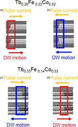
Reversal of current-induced domain wall motion in TbFeCo ferrimagnetic thin films across the magnetization compensation point
M. Ishibashi, K. Yakushiji, M. Kawaguchi, A. Tsukamoto, S. Nakatsuji, M. Hayashi, Jpn. J. Appl. Phys. 62, 013001 (2023).
We report on a systematic investigation of current-induced domain wall motion in TbFeCo ferrimagnetic thin films with a Pt underlayer. The Tb concentration of the alloy is varied to study the effect of the magnetization compensation on the current-induced motion of domain walls. We find that the direction in which domain walls move changes when the Tb concentration crosses the magnetization compensation point. Interestingly, the domain walls move along (against) the current flow for FeCo-rich (deficient) films. When the film composition is slightly Tb-rich than the magnetic compensation point, the domain wall moves along the current at a lower current but reverses its direction when the current is increased. These results suggest that two competing torques act on the domain walls in the Tb-based ferrimagnets (TbFeCo), causing the domain wall velocity to be more than one order of magnitude smaller than that of Gd-based ferrimagnets.

© 2023 The Japan Society of Applied Physics
Piezomagnetic switching of the anomalous Hall effect in an antiferromagnet at room temperature
M. Ikhlas, S. Dasgupta, F. Theuss, T. Higo, S. Kittaka, B. J. Ramshaw, O. Tchernyshyov, C. W. Hicks, S. Nakatsuji, Nat. Phys. 18, 1086 (2022).
Piezomagnetism couples strain linearly to magnetic order, implying that it can produce and control magnetization. However, unlike magnetostriction, which couples magnetization quadratically to strain, it enables bidirectional control of a net magnetic moment. If this effect becomes large at room temperature, it may be technologically relevant, similar to its electric analogue, piezoelectricity. However, current studies of the piezomagnetic effect have been primarily restricted to antiferromagnetic insulators at cryogenic temperatures. Here we report the observation of large piezomagnetism in the antiferromagnetic Weyl semimetal Mn3Sn at room temperature. This material is known for its nearly magnetization-free anomalous Hall effect. We find that a small uniaxial strain on the order of 0.1% can control both the sign and size of the anomalous Hall effect. Our experiment and theory show that the piezomagnetism can control the anomalous Hall effect, which will be useful for spintronics applications.

© The Author(s), under exclusive licence to Springer Nature Limited 2022
Perpendicular full switching of chiral antiferromagnetic order by current
T. Higo, K. Kondou, T. Nomoto, M. Shiga, S. Sakamoto, X. Chen, D. Nishio-Hamane, R. Arita, Y. Otani, S. Miwa, S. Nakatsuji, Nature 607, 474 (2022).
Electrical control of a magnetic state of matter lays the foundation for information technologies and for understanding of spintronic phenomena. Spin–orbit torque provides an efficient mechanism for the electrical manipulation of magnetic orders. In particular, spin–orbit torque switching of perpendicular magnetization in nanoscale ferromagnetic bits has enabled the development of stable, reliable and low-power memories and computation. Likewise, for antiferromagnetic spintronics, electrical bidirectional switching of an antiferromagnetic order in a perpendicular geometry may have huge impacts, given its potential advantage for high-density integration and ultrafast operation. Here we report the experimental realization of perpendicular and full spin–orbit torque switching of an antiferromagnetic binary state. We use the chiral antiferromagnet Mn3Sn (ref. 17), which exhibits the magnetization-free anomalous Hall effect owing to a ferroic order of a cluster magnetic octupole hosted in its chiral antiferromagnetic state. We fabricate heavy-metal/Mn3Sn heterostructures by molecular beam epitaxy and introduce perpendicular magnetic anisotropy of the octupole using an epitaxial in-plane tensile strain. By using the anomalous Hall effect as the readout, we demonstrate 100 per cent switching of the perpendicular octupole polarization in a 30-nanometre-thick Mn3Sn film with a small critical current density of less than 15 megaamperes per square centimetre. Our theory reveals that the perpendicular geometry between the polarization directions of current-induced spin accumulation and of the octupole persistently maximizes the spin–orbit torque efficiency during the deterministic bidirectional switching process. Our work provides a significant basis for antiferromagnetic spintronics.

© The Author(s), under exclusive licence to Springer Nature Limited 2022
Anomalous Hall effect in nanoscale structures of the antiferromagnetic Weyl semimetal Mn3Sn at room temperature
T. Matsuo, T. Higo, D. Nishio-Hamane, S. Nakatsuji, Appl. Phys. Lett. 121, 013103 (2022).
The magnetic Weyl semimetallic state in the chiral antiferromagnet Mn3Sn has attracted interest for its potential in memory technology. Despite vanishingly small magnetization, the material exhibits large transverse responses that can be electrically manipulated, similar to ferromagnets. Through deposition on heated Si/SiO2 substrates, we have fabricated polycrystalline Mn3Sn films that have coarse surfaces, the thinner of which have a discontinuous structure comprised of grains with diameters of the order of 100 nm. We confirm that these grains retain the anomalous Hall effect arising in the time reversal symmetry broken chiral antiferromagnetic phase of Mn3Sn at room temperature by serially connecting the grains with an additional conducting layer. These results pave the path for the potential applications of nanoscale Mn3Sn systems, which could be useful in the development of energy efficient memory devices.


© 2022 Author(s). Published under an exclusive license by AIP Publishing.
Large Hall Signal due to Electrical Switching of an Antiferromagnetic Weyl Semimetal State
H. Tsai, T. Higo, K. Kondou, S. Sakamoto, A. Kobayashi, T. Matsuo, S. Miwa, Y. Otani, S. Nakatsuji, Small Sci. 1, 2000025 (2021).
Developing a technology to electrically manipulate a Weyl semimetal state is a vital step for designing a nonvolatile memory using topologically robust properties. Recently, such manipulation is realized for the first time in the antiferromagnetic Weyl semimetal Mn3Sn using the readout signal of anomalous Hall effect in the Mn3Sn/heavy metal (Pt, W) heterostructures. Here, it is reported that the switching of Hall signal can be significantly enhanced by 1) removing the buffer layer of Ru to adjust the crystal orientation of Mn3Sn, and 2) annealing after deposition of the heavy metal to change the interfacial condition. The switching of the Hall resistance is 0.35 Ω in the Mn3Sn/W sample, which becomes one order of magnitude larger than the previously reported value using Ru/Mn3Sn/Pt heterostructures. Moreover, by increasing the read current, it is found that the readout voltage may go well beyond 1 mV, a milestone for future applications in memory technology.

© 2021 The Authors. Small Science published by Wiley-VCH GmbH